PCB designPart 3 of 4Drawing 16.3 of 47
Version 3
Drawn from scratch with an LED under every key. It went wireless, and now it's going back to wired.
- StatusProduction, 2026. Version two built, version four drawn
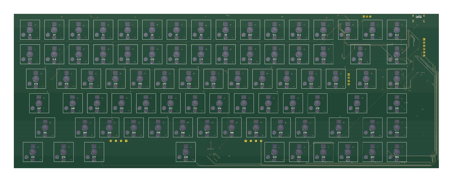
- Layout75%, 84 keys, hotswap Kailh Choc sockets
- Version twoSTM32F072 over USB-C, QMK with VIA, all 84 keys tested
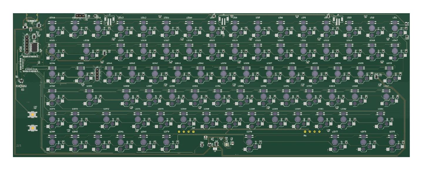
- Version threeper-key RGB, moving from wireless to wired
- Version fourTouch Bar, five PCBs, trackpad and numpad modules
- Softwaremy own Keyboard Editor app for remapping
Sheet 02 of 04/Gen3
Drawn from scratch
The third one I drew from scratch, with an addressable LED under every key.
Sheet 03 of 04/Going wireless
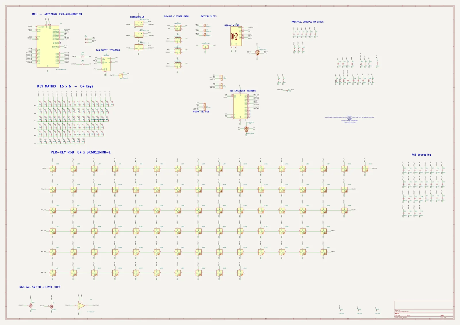
Wireless, then wired again
The third board went wireless on an nRF52840, which added chargers, battery slots and a power path between them and USB. It's now being converted back to a wired STM32 running QMK, so the key array stays and the power section gets redrawn.
Sheet 04 of 04/Gen3 trackpad
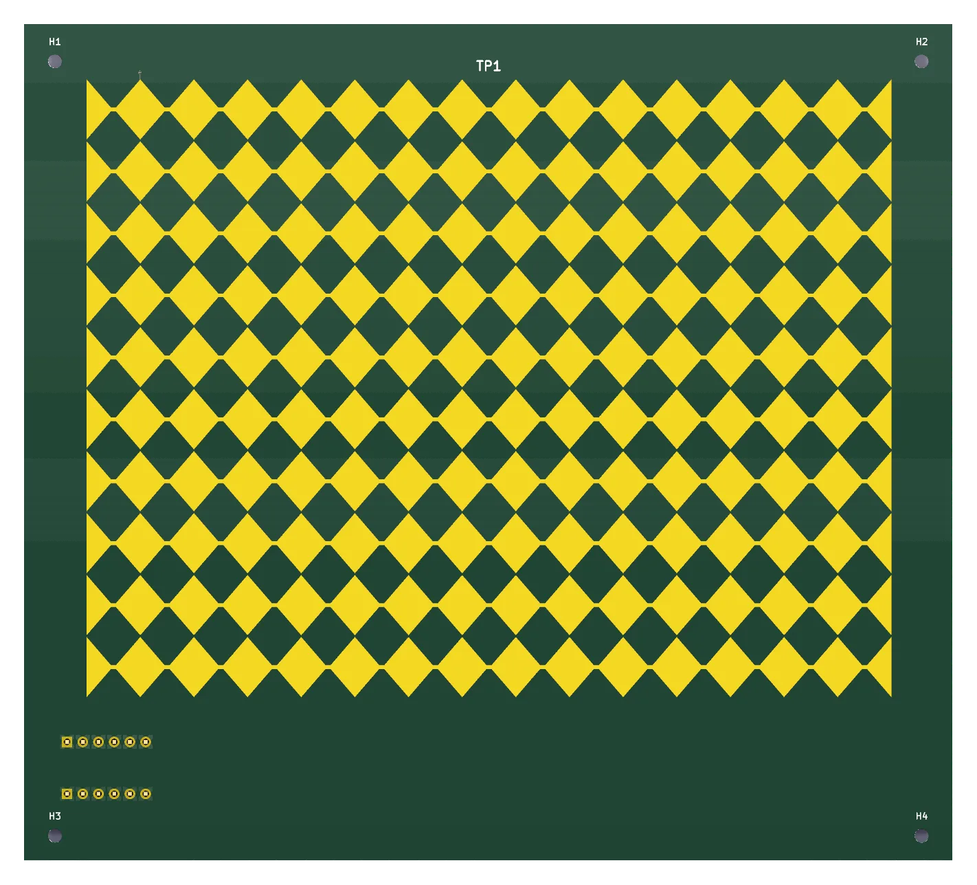
A detachable trackpad
The third board also got a trackpad module that connects through a six-pin pogo connector. It's placed and passes its checks, but the sensor isn't routed yet.